
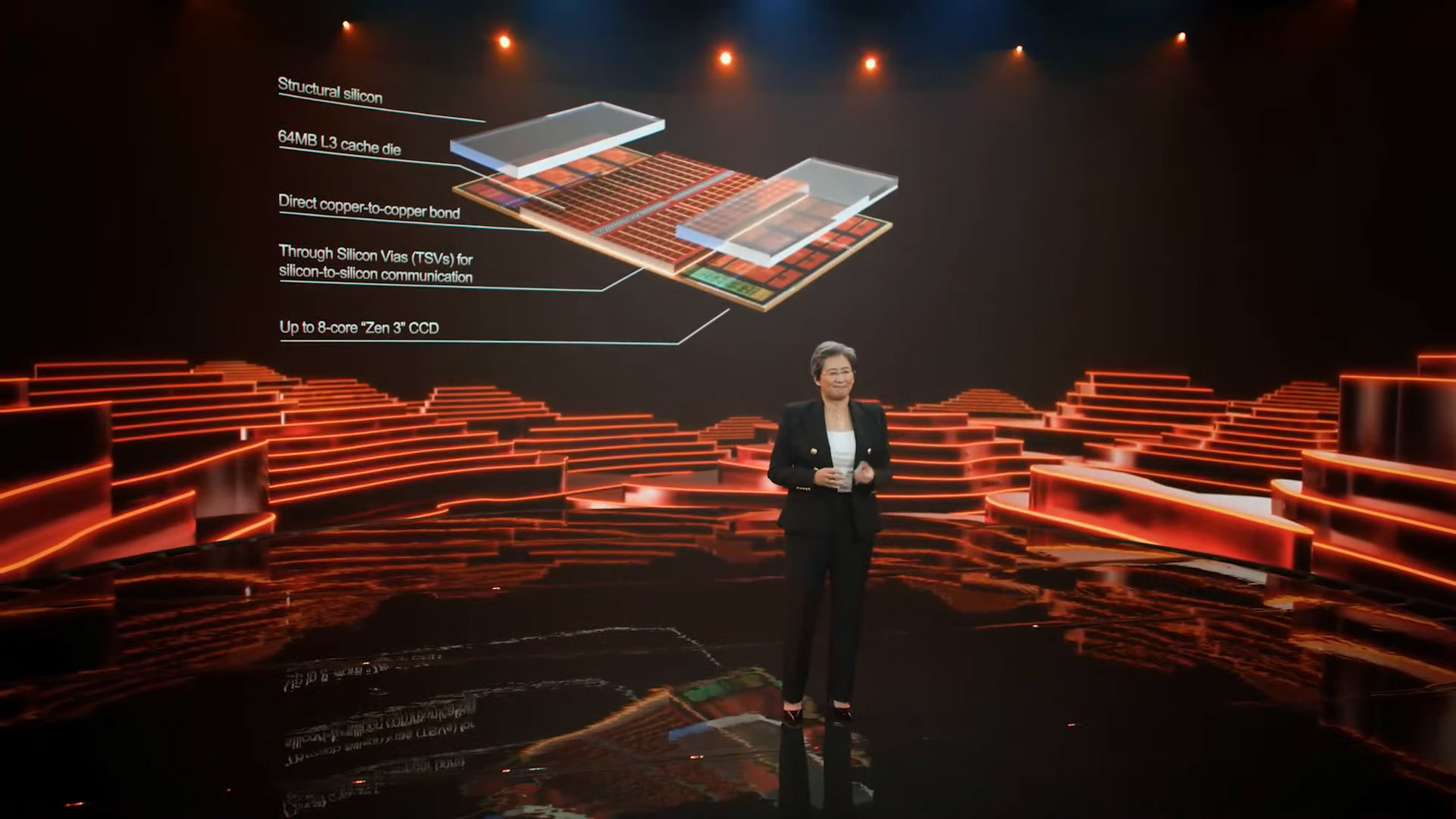
AMD CEO Lisa Su at Computex showed a sample of a twelve-core processor with Zen 3 cores, which carries a 64MB L3 cache layered on each processor chiplet. It reaches an area of 6 × 6, ie 36 square millimeters.
The cache environment is filled with inactive silicon only for chiplet alignment. Thinned silicon is used for both the chiplet itself and the layered L3 cache, so that current encapsulation technology can be maintained and higher enclosures are not required.
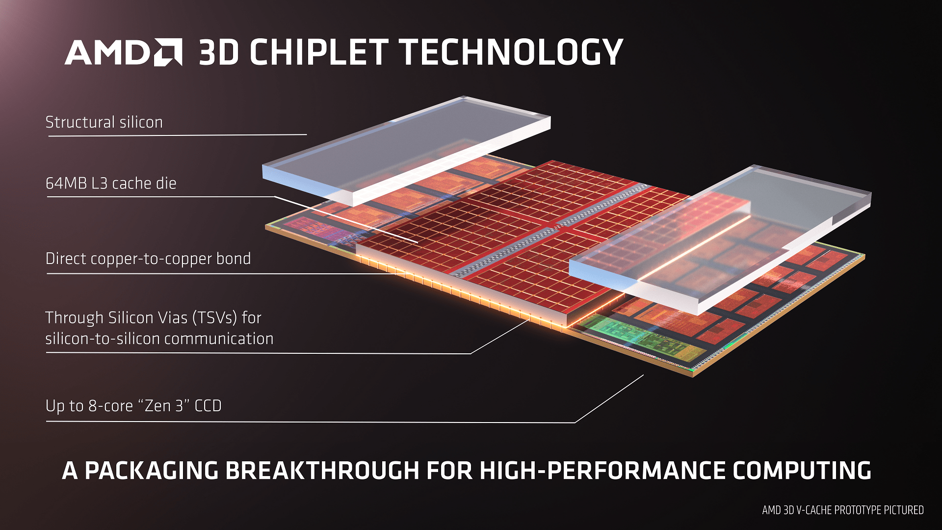
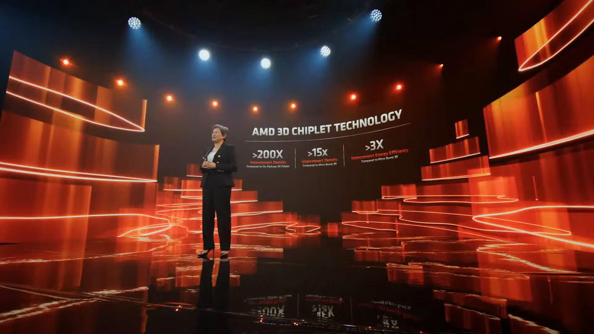
Chip on Wafer / Silicon on Silicon technology is used to connect the chiplet to the L3 cache layer, which achieves> 200 × higher connection density (ie wider bus),> 15 × higher connection density compared to Micro Bump technology used e.g. Intelen in the Foveros project / Lakefield and> 3x higher interconnection energy efficiency compared to Micro Bump. Thanks to such a wide bus, the added L3 cache achieves data throughput of over 2 TB / s, which exceeds the throughput of the L1 cache, but the latencies remain common for L3 cache.
Su presented performance results in games tested in 1080p resolution on the Ryzen 9 5900X and a similar processor with a layered + 2 × 64 MB L3 cache (192 MB total); for both processors with a set stable clock frequency of 4 GHz. The average game performance increased by 15%, which corresponds to a generational leap.

Lisa Su has confirmed that the technology will be used in production later this year for unspecified high-end products. It can be Epyc server processors, it can be high-end models of Ryzen processors. In this context, it already seems quite understandable that AMD could afford to cancel the 6nm half-generation Zen 3+ / Warhol. There were two alternatives, between which she chose and the choice probably fell on 3D chipsets.
Returning to the Epics, in the context of which we informed you about the deployment of layered chiplets last week, the situation basically turned out according to the most probable scenario:
| Probably the simplest would be to layer SRAM on existing or modified chipsets, thus avoiding the purchase of HBM from an external supplier, pads and more complex enclosures. That, of course, is just speculation. But it will probably not take long and we will find out more details. |
Epycu was concerned with the information that a series of 3D chiplets will carry up to ~ 1GB of cache. In the context of the above information, this seems like an easy-to-implement step: Ryzen, shown by Lisa Su, carried a 64 MB L3 cache layered on the chiplet, which took up 36 mm², which is not even half the area of the chiplet. Therefore, AMD can deploy 128MB of L3 cache in the server segment, with which we get to a total of 1024 MB of added L3 cache in eight chipsets per processor. So to that 1 GB.

If AMD wanted to implement this 1 GB via HBM, it would have to prepare a special chiplet with an interface for HBM to connect a 1GB HBM2 chip, connect it to HBM via a silicon pad (interposer) and the result would be 1GB cache with data throughput ~ 300 GB / s . With the alternative that AMD used, ie SRAM layering, it has 1GB cache even without the need for an interposer, without memory manufacturer margins and with data throughput of 4 × ~ 2 TB / s, ie 8 TB / s, which is about 26 times faster solution than using 2 , 4GHz HBM2.
–

