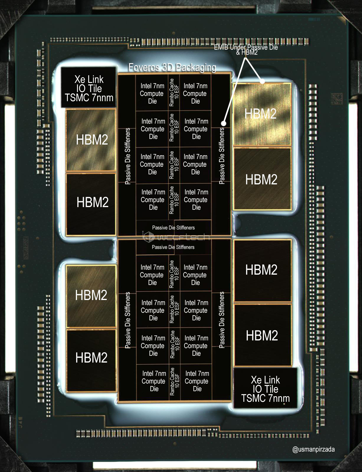
Earlier, Intel Chief Architect Raja Koduri shared the package photos of the Xe HPC GPU with the “seven-in-one” design, and then foreign media quickly analyzed the specifications of this dual-Tile GPU product using the 7nm process. The latest news is that WCCFTech quoted a source from the source and gave a chip chart with correct annotations, including the computing unit in the middle of the substrate, the HBM2 high-bandwidth display memory on both sides, and the Xe Link IO at the edge.
Previously, everyone’s understanding of the so-called “seven technologies” disclosed by Raja Koduri included the Foveros technology used by the dual-tile version of Xe HPC GPU, Intel’s 10nm ESF process, and TSMC’s 7nm process. Now through cross-confirmation with at least two sources, WCCFTech finally knows the correct annotations for the company’s first 7nm Xe HPC GPU chip package.
The first is the two Xe Link IO chips located in the upper left and lower right corners of the picture, which are manufactured using TSMC’s 7nm process. What is interesting is that two different sizes of HBM2 high-bandwidth display memory are also integrated on both sides of the substrate. The second is the Intel 7nm computing core located in the middle of the rectangular substrate. The 8 computing cores in each tile are integrated through Passive Die Stiffeners and connected to the HBM2 high-bandwidth display memory.
Obviously, in order to create this 7nm product, Intel has also applied technologies such as Embedded Multi-chip Interconnect Bridge (EMIB) and Foveros 3D packaging, as well as the 7nm IO connection chip and Rambo Cache manufactured by TSMC.
The following is a complete explanation of the “seven technologies” shared by Raja Koduri:
● Intel 7nm process;
● TSMC 7nm process;
● Foveros 3D package;
● EMIB embedded multi-chip interconnection bridge;
● Enhanced Super Fin manufacturing process;
● Rambo Cache;
● HBM2 high bandwidth display memory;
–


