Heat
Earlier this week, as AMD began to rumor that AMD was planning to deploy layered chips, and it looked like a cache layered on chips, users were worried about how AMD would handle heat. First of all, it must be said that silicon is not a bad conductor of heat, on the contrary, it is equal to the thermal conductivity of many metals. The thermal conductivity is more temperature dependent than most metals, but at the temperature normally reached by x86 processors under load (according to various sources 120-175 W / m K) it is higher than the thermal conductivity of iron and comparable to zinc or brass.
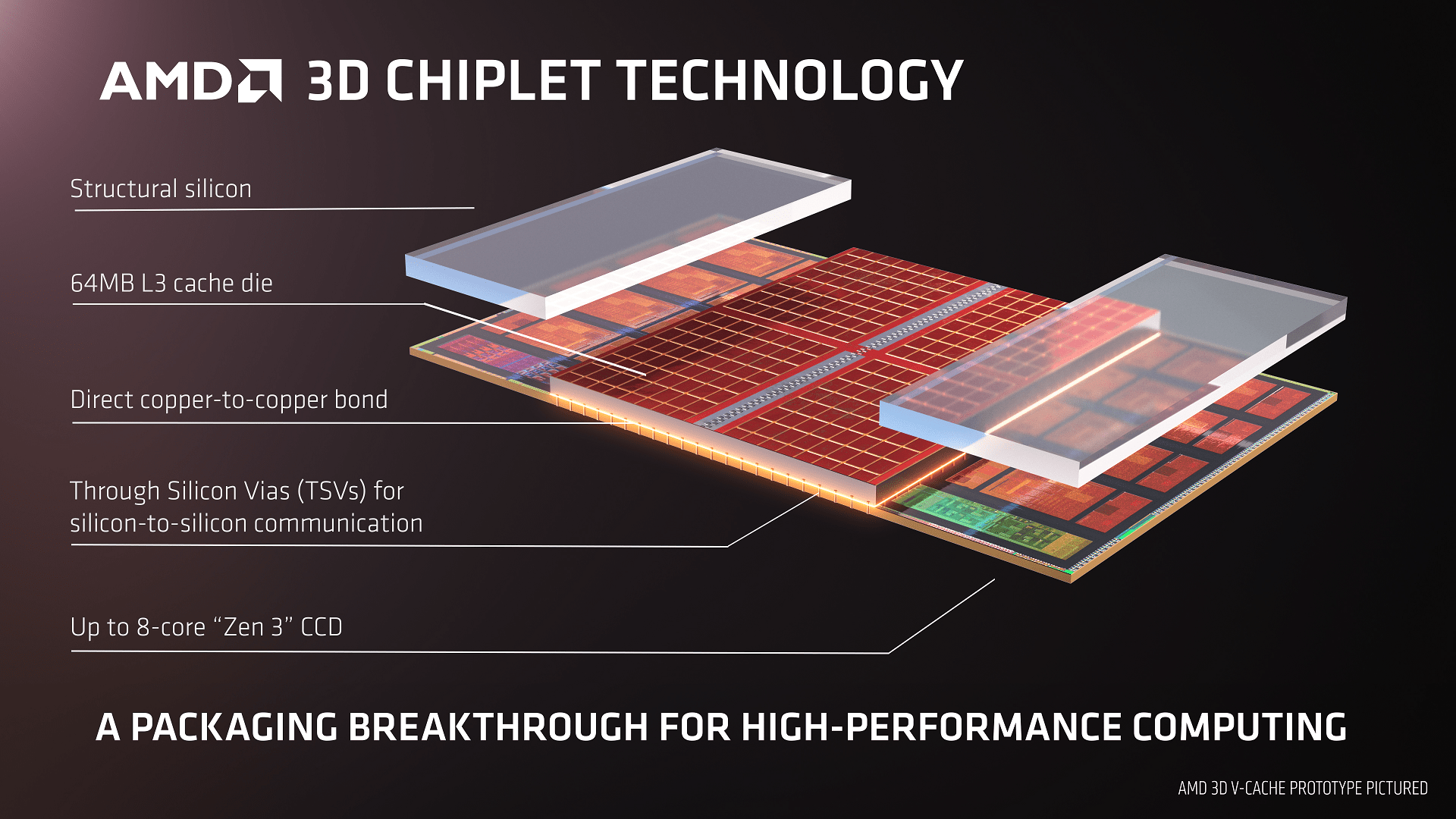
In the case of the demonstrated desktop Ryzen, where “only” 64 MB per chiplet is used, which corresponds to dimensions of 6 × 6 millimeters, the cache layer does not overlap the x86 cores themselves. In the image of the Zen 3 chiplet described below, I marked (with a white frame and a colorless surface) an area that corresponds to the layered cache. It overlaps the native L3 cache and part of the L2 cache – the processor cores do not cover the cache:
But take the location as an illustration. It is clear that the situation is not as nice as it is painted on the official slide in the introduction – the chiplet is about 7.3 millimeters wide and the cache 6 millimeters, so about 1.3 millimeters remains uncovered. Whether this corresponds to the GMI interface, as I indicated in the picture, is not known (but it would make quite sense).
The rest of the chiplet is covered by silicon without logic so that heat can be transferred from it to the IHS and heatsink. It should be silicon modified for higher thermal conductivity, but nothing more has been published. However, the thermal conductivity of this silicon cannot be expected to be drastically better – perhaps by a few tens of percent. Anyway, nothing fundamental that would mean a break. Personally, I consider that for server processors (Milan-X), where the amount of waste heat per chiplet is more significantly limited, there will be no problem if the entire chiplet is covered (128MB) L3 cache.
This should not be a problem from the principle, because to maintain the height of the central chiplet and the whole case, thin silicon is used for x86 chipsets and layered L3 cache, so the height of the whole silicon structure (chiplet + layered L3 cache) is the same as for contemporary unlayered chips. As a result, the layer of silicon that heat must pass through is not a tenth of a millimeter higher than current processors.
Importance
AMD boasted of presenting gaming performance, which usually benefits relatively well from CPU cache capacity. For other types of tasks where caching could occur, the main candidates for the task are data compression. The video compression is probably less, as it is designed with respect to blocks using algorithms so that the blocks fit into the standard cache.
Overall, however, a wider application can be expected in the professional sphere, where much larger data volumes are processed. Tasks where it is not possible to divide the data into very small blocks or this division has certain limitations could show a significant increase in performance.
If we realize that AMD on a 12-core desktop model illustrated the possibility of equipping the game processor with 192MB of memory (L3 cache), one cannot nostalgically remember the legendary Diablo II, which required more than 128 MB of RAM for a decent run. On the Ryzen demo, all the necessary data would fit in the L3 cache and the user would no longer have to worry about the operating memory.
Application
AMD demonstrated the technology on Ryzen, a desktop processor. Because it boasted of gaming performance, it can be assumed that desktop Ryzens equipped with this cache will be mass-produced and released. But we also know (although this has not been officially confirmed on Computex; it is possible that AMD keeps it on HotChips or another opportunity) that the layered chipsets will also be used by the server. Milan-X.
It has been confirmed that layered cache processors will be mass-produced later this year. AMD did not explicitly state that it would be a desktop series, but it would follow from the context (there was no other language). Unofficial sources spoke of the likely release of the layered Milan-X by the end of the year, so it is possible that the technology will be available for servers in the fourth quarter and the desktop will follow shortly thereafter; the launch could take place in January at CES 2022, which would also be a response to Intel Alder Lake, which is expected to be available at the end of the year, around November.
In addition to desktops and servers, there are also considerations about the mobile segment, which are primarily APUs. But there, according to leaker Bondrewd v-cache deployment is not planned in the foreseeable future. This makes sense, as a thinned design is already used for mobile processors and no increase would be desirable. The APU should use SLC cache, common cache for CPU and GPU kernels in the future. It will probably be part of the basic silicon and will probably come in an era Zen 4.
–


