Commercialization of artificial intelligence HBM-PIM… Equipped with AI calculation function in memory semiconductor
Double the performance compared to existing products… Publication of thesis at ISSCC
Samsung Electronics developed the world’s first intelligent memory semiconductor technology that changes the paradigm of existing memory semiconductors.
It is a technology that allows memory not only to be stored but also to some operations by mounting an artificial intelligence (AI) engine on a memory semiconductor that was considered only as a data storage space.
–
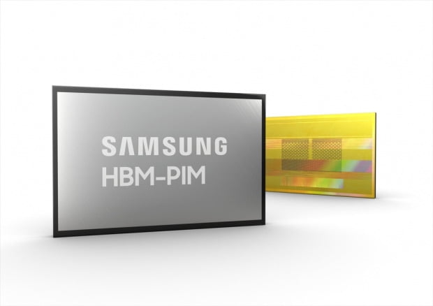
Samsung Electronics announced on the 17th that it has developed the world’s first HBM-PIM (Processing-in-Memory) product that combines a memory semiconductor and an artificial intelligence processor.
PIM refers to a next-generation new concept convergence technology that adds processor functions necessary for computing tasks inside the memory.
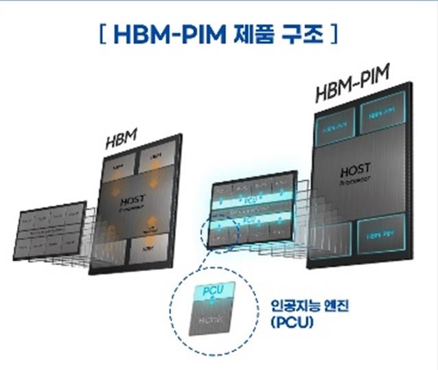
Using PIM technology, Samsung Electronics developed HBM-PIM equipped with an artificial intelligence engine on HBM2 (High Bandwidth Memory) Aquabolt, which is used for ultra-high-speed data analysis such as supercomputer (HPC) and AI.
HBM2 Aquavolt is a second-generation high-bandwidth memory semiconductor mass-produced by Samsung Electronics in January 2018.
According to Samsung Electronics, when HBM-PIM is installed in an AI system, the performance of the system using the existing HBM2 is approximately doubled and the system energy is reduced by more than 70%.
In addition, customers who use HBM by supporting the existing HBM interface can build a powerful AI accelerator (dedicated hardware for executing artificial intelligence) system using HBM-PIM without changing hardware or software.
Recently, as the application area of artificial intelligence has been expanded and technology has been advanced, the demand for high-performance memory has continuously increased, but it has been difficult to overcome the limitations of the’fon Neumann’ structure with the existing memory.
The von Neumann structure is a method used in most computers, in which the central processing unit (CPU) loads and executes instructions from the memory, and stores the results in the storage device sequentially.
In this process, if the amount of data exchanged between the CPU and the memory increases, the work processing is delayed.
To overcome this, Samsung Electronics installed an artificial intelligence engine in each bank (the smallest logical unit when composing the main memory) in the memory and maximized parallel processing to increase performance.
In addition, HBM-PIM can process calculations inside the memory, reducing data movement between the CPU and memory, thereby increasing the energy efficiency of the AI accelerator system.
 –
–
–
Samsung Electronics has succeeded in commercializing HBM-PIM by incorporating this technology into the DRAM process, and recently released a related paper at ISSCC, the world’s top academic society in the semiconductor field.
“HBM-PIM is the industry’s first customized PIM solution that can maximize the performance of AI accelerators,” said Park Kwang-il, head of the product planning team at Samsung Electronics’ memory division. Will continue to build.”
In the first half of the year, Samsung Electronics plans to complete test verification by mounting HBM-PIM in AI accelerators of various customers.
A Samsung Electronics official said, “HBM-PIM is expected to be adopted as an AI accelerator for the first time, and it will be able to expand its application to general products such as smartphones through future technology development.”
/yunhap news
–


